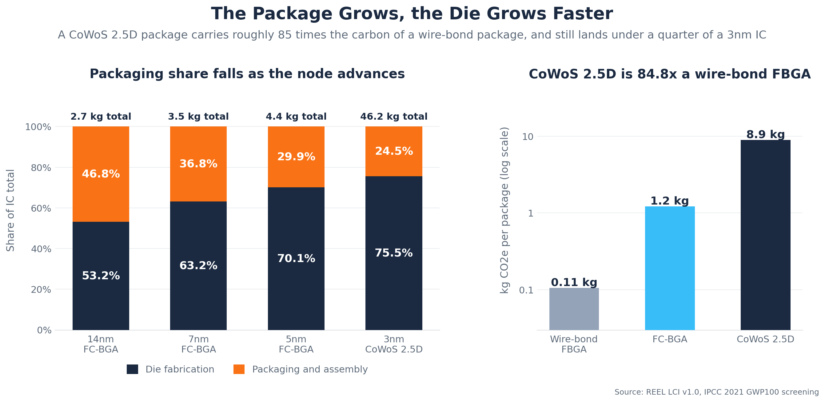
A CoWoS 2.5D package carries about 85 times the carbon of a wire-bond FBGA package. On an advanced-node chip, it is still the smaller of the two terms.
The figures below are screening results from REEL LCI v1.0 (released 21 August 2026), characterised with IPCC 2021 GWP100 factors. They are screening-level numbers, so read the direction rather than the third digit.
When AMD, Intel, and NVIDIA split their designs into chiplets, smaller dies connected through advanced packaging, they get better yields, faster design cycles, and the ability to mix and match process nodes. Smaller dies mean fewer defects per die, which means higher yield, which means less wasted silicon. That is a real improvement of semiconductor economics.
The packaging side of that math gets less attention, and in absolute terms it is a large step up. Silicon interposers, redistribution layers, and through-silicon vias look a lot like a second semiconductor manufacturing process. In v1.0, a wire-bond FBGA package screens at 0.105 kg CO2e per package and a flip-chip BGA at 1.21 kg, while a CoWoS 2.5D package screens at 8.92 kg. That is 84.8 times the wire-bond package, and roughly seven times the flip-chip BGA.
Set that against the die it carries, though, and the ranking flips. The 3nm IC on CoWoS 2.5D screens at 46.2 kg CO2e in total: 34.9 kg for die fabrication and 11.3 kg for the package and assembly. Even with an interposer under it, packaging is 24.5% of the chip.
The direction across nodes is the part that probably matters most for design decisions. On the three monolithic flip-chip BGA faces, the package term barely moves, 1.28 to 1.30 kg, while the die term climbs from 1.46 kg at 14nm to 2.24 kg at 7nm and 3.05 kg at 5nm. So the packaging share falls: 46.8% at 14nm, 36.8% at 7nm, 29.9% at 5nm, and 24.5% for the 3nm part on its interposer. Mature-node parts in small packages sit in a similar band, between 12.8% for a 180nm PMIC in a QFN and 31.6% for a 180nm op-amp in an SOIC-8. Advanced packaging is not what pushes packaging up the contribution list; an expensive die is what pushes it down.
Two caveats on the comparison. The 3nm face carries a 600 mm² die, while the flip-chip BGA faces carry 100 to 120 mm² dies, so part of that last step is die area rather than node. And v1.0 does not model one product twice, once monolithic and once split into chiplets, so this is a comparison across separate faces rather than a controlled A/B of a single design.
What the numbers seem to be saying is that the interesting question for a chiplet program is not whether the package overtakes the die. On advanced nodes it probably does not. The question is whether splitting a large die into chiplets buys enough yield and enough usable silicon area to pay for an interposer that costs tens of times a conventional package. At 8.92 kg per package, a 2.5D interposer is worth about two whole 5nm monolithic parts on its own, which is a real budget to recover through yield.
The chiplet tradeoff, at least as v1.0 sees it, looks like cost against performance against a packaging line item that is now big enough to design around.