A standard DRAM chip and an HBM stack are built from the same thing: fabricated silicon. What separates them is how much of it each one carries.
In REEL LCI v1.0 (released 21 August 2026), a standard 1-alpha DRAM IC in a wire-bond FBGA package comes to about 0.53 kg CO₂e. An HBM3 8-Hi stack, 16 GB, comes to about 13.5 kg. That is roughly 25 times as much embodied carbon, and about 85% of it is wafer fabrication: 75% for the eight thinned core DRAM dies, another 10% for the base logic die underneath them. TSV stacking, die thinning and precision assembly together account for about 15%.
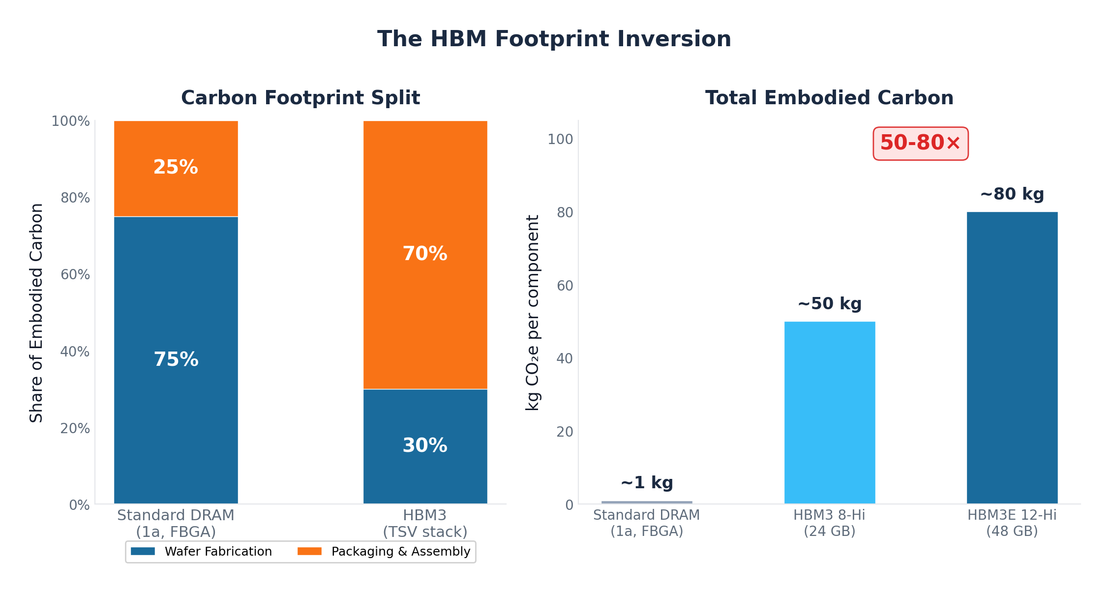
So the step that makes HBM distinctive, drilling thousands of through-silicon vias, filling them with copper and bonding dies thinned to 40 micrometers with sub-micron alignment, is not where most of the carbon lands. The stacking process is energy-intensive in its own right, but in this screening it is a modest slice of the total. The dominant term is die area: many more dies, larger dies, and a logic die built on a different process than the memory above it.
The v1.0 screening figures, IPCC 2021 GWP100, per component:
- Standard 1-alpha DRAM IC, 8 Gb, wire-bond FBGA: 0.53 kg CO₂e (80% wafer, 20% package)
- HBM3 8-Hi stack, 16 GB: 13.5 kg CO₂e (85% wafer, 15% stacking)
- HBM3 12-Hi stack, 24 GB: 19.8 kg CO₂e (87% wafer, 13% stacking)
- HBM3E 12-Hi stack, 36 GB: 20.6 kg CO₂e (87% wafer, 13% stacking)
That is a 25x to 39x range from a standard DRAM chip to an HBM stack, and the spread within HBM tracks die count and die size rather than the packaging route. Going from 8-Hi to 12-Hi adds four more core dies and moves the total by about half again; the stacking share actually falls, from 15% to 13%, because the added dies grow the wafer term faster than they grow the assembly term.
For anyone estimating the embodied carbon of AI servers, GPUs or data center hardware, two things follow. First, memory is a large share of the component-level footprint: a GPU carrying six HBM3E 12-Hi stacks carries roughly 124 kg CO₂e in the memory alone. Second, if you are trying to reduce that number, the levers that matter are the ones that change silicon area and the fabs it comes from, capacity per die, yield, the process node of the base die and the grid mix where the wafers are made. Optimizing the stacking step moves a 15% slice.
It also means "DRAM" is not a useful single category for this purpose. Two parts with the same three letters on the datasheet differ by more than an order of magnitude in embodied carbon, and the difference is mostly silicon, not assembly. Modelling memory by capacity alone, or by a single average per gigabyte, will miss it in either direction.
These are screening-level results: a GWP100 characterization run over the REEL v1.0 inventory, useful for ranking and for order-of-magnitude work, not a substitute for a full assessment of a specific part. The underlying inventories, and the stacking model with its 40 micrometer die thinning, are in the database.