A 40-layer backplane PCB has roughly 11 times the carbon footprint of a standard 4-layer board.
Not 10 times the layers. More than 11 times the carbon. Because PCB fabrication doesn't scale linearly at high layer counts.
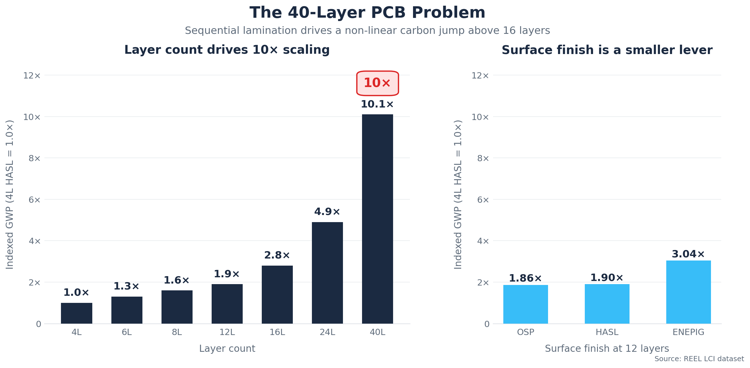
Here's the full scaling curve from the REEL LCI dataset, indexed to a standard 4-layer FR-4:
- 4L: 1.0x
- 6L: 1.1x
- 8L: 1.5x
- 12L: 2.3x
- 16L: 3.1x
- 24L: 5.8x
- 40L: 11.4x
Up to about 16 layers, the relationship is roughly linear. Above that, it accelerates – driven by sequential lamination processes. You can't press 40 layers at once. You build sub-stacks, laminate, drill blind vias, plate, then build more sub-stacks on top. Each sequential cycle adds its own etching, imaging, plating, and testing steps.
Electricity is the single largest contributor at 37–58% across configurations, but it is not what accelerates. Electricity per m² rises about 8-fold from 4 to 40 layers, while copper foil rises roughly 35-fold. Above 16 layers the curve is bent by conductor mass, not by the fab.
Surface finish adds another dimension. For a 12-layer server PCB, the difference between the cheapest finish (OSP, 1% below HASL baseline) and the most expensive (ENEPIG, 15% above HASL) is significant in absolute terms – but it's still less than the gap between a 12-layer and 24-layer board of the same finish type.
For screening-level assessments: layer count is the parameter that matters. Surface finish is secondary unless you're specifying palladium- or gold-containing options.
For data center and networking hardware teams: those 24-layer and 40-layer switch and backplane PCBs are not environmentally negligible. They're a meaningful fraction of the board-level embodied carbon.